11/24/2009

CSIRO to launch GPU-based supercomputer


By Brett Winterford
Nov 23, 2009 12:23 AM
Tags: csiro | gpu | nvidia | teraflops | supercomputer | cluster
Uses GPU cluster to trump machines twice its size.
The CSIRO is expected to this week announce the launch of a new supercomputer, which uses a cluster of GPUs (graphical processing units) to gain a processing capacity that competes with supercomputers over twice its size.
The supercomputer is one of the world's first to combine traditional CPUs with the more powerful GPUs.
According to the updated CSIRO website it has 128 Dual Xeon E5462 Compute Nodes (i.e. a total of 1024 2.8GHz compute cores) with 16 GB or 32 GB of RAM, 500 GB SATA storage and DDR InfiniBand interconnect. And it has 64 Tesla S1070 - 256 GPUs with 61440 streaming-processor cores.
The supercomputer has 144-port DDR InfiniBand Switch and an 80 Terabyte Hitachi network attached storage file system.
The CSIRO said the supercomputer 's NVIDIA-based GPU technology can increase the speed of its scientific data crunching by a factor of between 10 and 100.
The CSIRO claimed the system boasted processing capacity of some 200+ teraflops (i.e. over 200 trillion floating point calculations per second), which would appear on face level to be greater than the 140 teraflop-capablesupercomputer announced by the Australian National University last week.
But the CSIRO concedes that these stats can't be taken on a like-for-like basis - the CSIRO supercomputer is 256 Teraflops of "single precision" (32-bit) computing performance, while the ANU machine is 140 Teraflops of"double precision" (64-bit) computing performance.
The CSIRO has more information on the GPU cluster here.
Stay tuned for more on the new supercomputer in this afternoon's edition ofiTnews.
The original version of this story working on pre-release information from the CSIRO incorrectly said that the supercomputer would have 100 Intel Xeon CPU chips and 50 Tesla GPU chips. The error was corrected in this version.

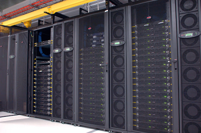
Inside the Datacentre pod with CSIRO GPU Cluster.

CSIRO GPU Cluster racks during installation, front view

CSIRO GPU Cluster racks during installation, front view

CSIRO GPU Cluster compute nodes

CSIRO GPU Cluster racks during installation.


CSIRO GPU Cluster racks during installation.

Datacentre pod with CSIRO GPU Cluster.

CSIRO GPU Cluster compute nodes Infiniband cabling and patch panel.

CSIRO GPU Cluster Hitachi data storage, front view

CSIRO GPU Cluster Hitachi data storage, rear view.

CSIRO GPU Cluster Hitachi storage controllers (HNAS)

Cluster Communication rack patch panels.


11/23/2009

OCZ Colossus SSD


more detail - http://www.pcper.com/article.php?aid=821&type=expert&pid=1

Fusion-io’s SSD Setup Reaches 1TB/s Aggregate Bandwidth.


Fusion-io, a designer of high-end solid-state drive (SSD) solutions, announced this week that it would deploy custom installations based on its ioMemory technology at two presently undisclosed government organizations. Each deployment consists of hundreds of terabytes of solid-state storage capacity and is capable of sustaining over 1TB/s of aggregate bandwidth with access latencies under 50ms.
The extreme performance achievements were made possible by Fusion-io’s development of the ioDrive Octal card, a custom PCI Express card. The device holds eight ioMemory Modules – putting the equivalent capacity and performance of eight ioDrives into a single card. The ioDrive Octal fits any PCI Express 2.0 x16 double-wide slot, the same as those used for high performance graphics cards, and it is capable of saturating the full performance of that slot. The ioDrive Octal again demonstrates the flexibility, performance and scalability of Fusion’s ioMemory architecture, the core technology that powers all the company’s enterprise products.
Achieving a 1TB/s sustained bandwidth with existing storage technologies requires close to 55 440 disk drives, 396 SAN controllers, 792 I/O servers and 132 racks of equipment. Fusion-io can achieve this same bandwidth with a mere 220 ioDrive Octal cards, housed in Infiniband-attached I/O servers running the Lustre parallel file system. This 1TB/s Fusion-io based solution requires six racks or less than 1/20th the rack space of an equivalent, high-performance, hard disk drive-based storage system.
“We were eager to take on the challenge of creating a device that meets the intense demands of high performance computing. With this architecture, IOPS are easy. We achieved over a hundred million IOPS, more than enough performance to meet our customer’s requirements. The real power in our architecture was the ability to also scale bandwidth. We look forward to productizing the ioDrive Octal in the future, and bringing the power of this solid-state storage technology from the world of HPC to the enterprise,” said Steve Wozniak, chief scientist at Fusion-io.
Specifications of ioDrive Octal look as follows:
  • 800,000 IOPS (4k packet size);
  • 6 GB/s bandwidth;
  • 5 TB maximum capacity;
  • PCIe x16 2.0 double-wide PCI Express form factor.
“Innovative technology, like Fusion's ioMemory, will fundamentally change the way the industry architects high performance computing facilities in the future. Technologies like these will drive new and emerging HPC systems as they continue their exponential growth in performance. Only improvements in storage bandwidth at this order of magnitude can keep the floor space and power consumption requirements from becoming unmanageable and unsustainable,” said Mark Seager, manager of the platforms program for the advanced simulation and computing (ASCI) program at Lawrence Livermore.


11/18/2009

OCZ officially unveils the Colossus 3.5-inch SSDs

Almost six months after their first sighting, the Colossus 3.5-inch solid state drives from OCZ have finally been announced. The 120GB, 250GB, 500GB and 1TB drives have an aluminum casing and feature MLC (multi-level cell) NAND flash memory chips, internal RAID, two controllers and 128MB of cache memory, a SATA 3.0 Gbps interface, a MTBF (mean time before failure) of 1.5 million hours, and deliver read and write speeds of up to 260 MB/s.

"The new Colossus Series is designed to boost desktop and workstation performance and is for high power users that put a premium on speed, reliability and maximum storage capacity," said Eugene Chang, VP of Product Management at the OCZ Technology Group. "The Colossus core-architecture is also available to enterprise clients with locked BOMs (build of materials) and customized firmware to match their unique applications."

The Colossus SSDs are backed by a three-year warranty and are said to start off at $300.


http://www.tcmagazine.com/comments.php?shownews=30976&catid=2

Multi-GPU Radeon HD 5000 series video card "Radeon HD 5970"

AMD is November 18, Radeon HD 5000 series GPU Multi-core video card is "Radeon HD 5970" announced. Radeon check the performance of the new flagship product. 

● Equipped with two full-spec based on the Cypress, the clock specification 5850


Hemlock had been predicted by the code name "Radeon HD 5970" is, Radeon HD 5000 series architecture based on multi-GPU is the video card. Radeon HD 3000/4000 generation, product name at the end of "X2" multi-GPU and it was put to clarify that the video card, this generation has shown that the Radeon HD 5800 series lineup top The model name is adopted.

AMD will use here is borrowed from the reference board, the board length is very long (photo 1,2). AMD multi-GPU on one PCB video card with two GPU put the style (Photo 3) and sticking to the board tend to be really long.


p1.jpg
[Photo 1] Radeon HD 5970 reference board


ph02.jpg
[Photo 2] long board is about to end, including the design of 310mm. Radeon HD 5870 more than 3cm long and is

ph03.jpg

[Photo 3] The back of the reference board. GPU single PCB to the two shows that are listed


The main specifications are as shown in Table 1. Once a brief, 20 SIMD units have enabled all of the Radeon HD 5870 for full-spec engine, the same group with two core Cypress, the clock will be called Radeon HD 5850 running at an equivalent product. AMD demonstrated its architecture in Figure 1 is a description of materials. PLX Techology Cypress Core 2 based chip will be connected by a bridge style. This is like the Radeon HD 4870 X2/3870 X2.


Table 1 Radeon HD 5970 Specifications


Radeon HD 5970Radeon HD 5870Radeon HD 5850
Process rules40nm 
Core clock725MHz850MHz725MHz
SP Number1,600 units × 21,600 units1,440 units
Texture Units80 units × 280 units72 units
Memory1GB × 2 GDDR51GB GDDR5 
Overclocking1,000 MHz1,200 MHz1,000 MHz
Memory Interface256bit × 2256bi t 
ROP Units32 units × 232 units 
Power Board (idle)42W27W 
Power Board (peak)294W188W151W


ph03_1.jpg

[Figure 1] Block diagram of the Radeon HD 5970


Incidentally, the reference board try to remove the cooler, GPU, and each of the two units can be sure that 1GB of GDDR5 memory and being (Photos 4-7). H5GQ1H24AFR-T2C on Hynix's memory, 5.0Gbps memory chip that supports up. 4.0Gbps say that there is enough for chips.


ph03_2.jpg
[Photo 4] after removing the air conditioner. Cypress both sides of the core GPU, the central bridge chips
ph03_3.jpg
 [Photo 5] each GPU connected to the memory of 8 total. Each per GPU, the surface of four sheets, the back four sheets to implement
 ph06.jpg
[Photo 6] The video memory is Hynix H5GQ1H24AFR-T2C. 1Gbit chips each GPU to eight pieces each, and a total of 2GB
 ph06_1.jpg

[Photo 7] Vapor Camber cooler is that adopted the thermal conductivity (transport) which increases


And have adopted such a memory, Radeon HD 5970 is a point that is also appealing design that is over with the clock (Figure 2-3). Power consumption, but later, 300W while running clock set to exceed the current frame that leaves room for the tune score, suggesting that the idea.


ph06_2.jpg
[Figure 2] Radeon HD 5970 is designed to appeal to the board with overclocking


ph06_3.jpg

[Figure 3] which also shows the design with the clock over here, in terms of features and structures, including a cooler


Bridge chip, ATI logo and "AMD8647-BBB50BC" was stamped the model number (photo 8). However, as was also the first document, the entity would PLX Technology products. AMD8647 and from the model show that, Radeon HD 4870 X2 like 48-lane PCI Express 2.0 bridge chip PEX8647 is believed to have been used.

294W peak power is in the way of the board, power supply terminal is equipped with 6-pin and 8-pin (Photo 9). PCI Express slots, +8 pin 6 can be supplied in-line configuration on the edge, and 300W power supply pin, the clock speed of the Radeon HD 5850 that is considerable and seems to be greater for this reason. The PEX8647 bridge chip, the product literature, 2.8W typical power consumption has been marked, Radeon HD 5970 from my total, and large enough to affect the power is not major.

Bracket of the Mini DisplayPort and DVI × 2 configuration is (photo 10). Eyefinity Radeon HD 5000 series features characteristic of these three can be used simultaneously to one output, Mini DipslayPort the availability of good points from the DisplayPort adapter to convert it disturbing. Most, Mini DisplayPort also finally standardized as the VESA standard so extended, the potential for improved high availability of these adapters.
 

ph06_4.jpg
[8] with two photos and GPU connection, PC with PCI Express bridge chip provides the interface "AMD8647-BBB50BC" use. PLX Technology is a chip made


ph09.jpg
[Photo 9] 6-pin power supply terminal pin configuration +8


 ph09_1.jpg

[10] pictures of the bracket DVI-I × 2 + Mini DisplayPort is and


In addition, Native CrossFire and pins, this product can be used two pieces Quad CrossFire (Photo 11). Rated as the clock is running when the idle core by ATI PowerPlay 157MHz, Memory 300MHz to ensure that the clock is down to (screen 1)
ph09_2.jpgph09_3.jpg